I spent some time trying to design a decent, low cost, reliable power supply for my workbench. It took quite a bit of time to get this right, and even then there are issues that still need to be addressed.
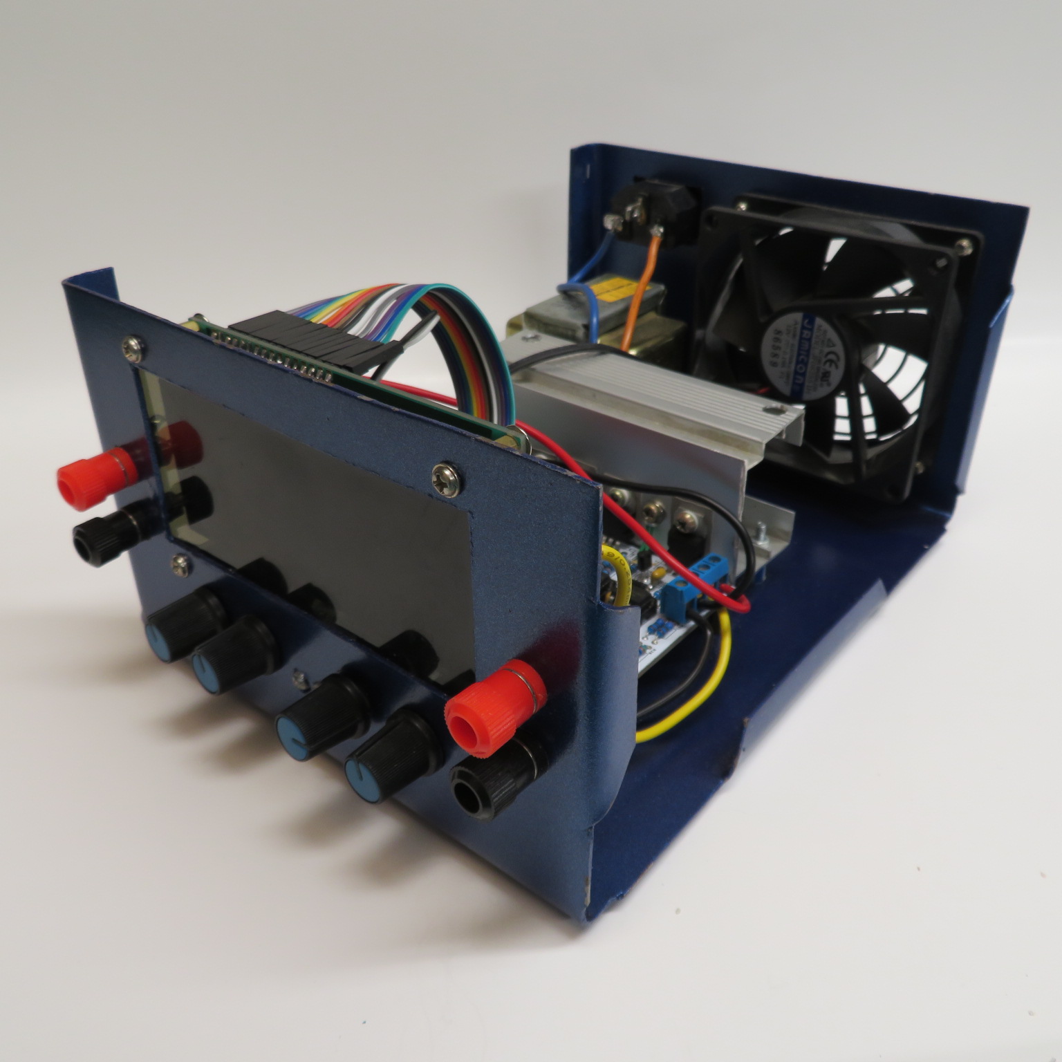
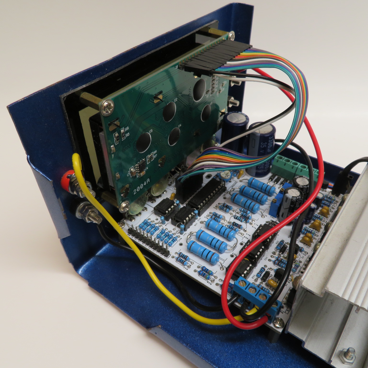
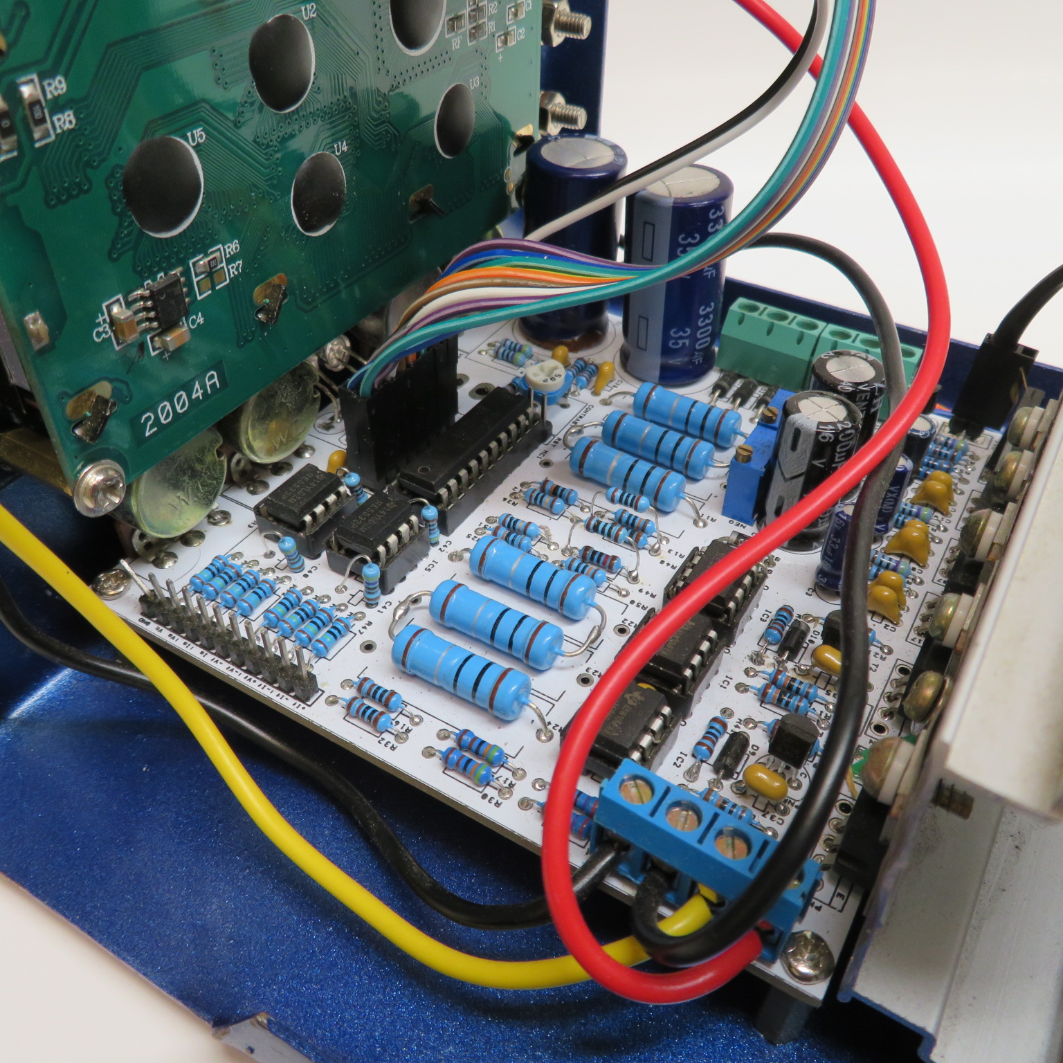
Here are some images of the inner guts of this thing. The board inside it the latest revision.
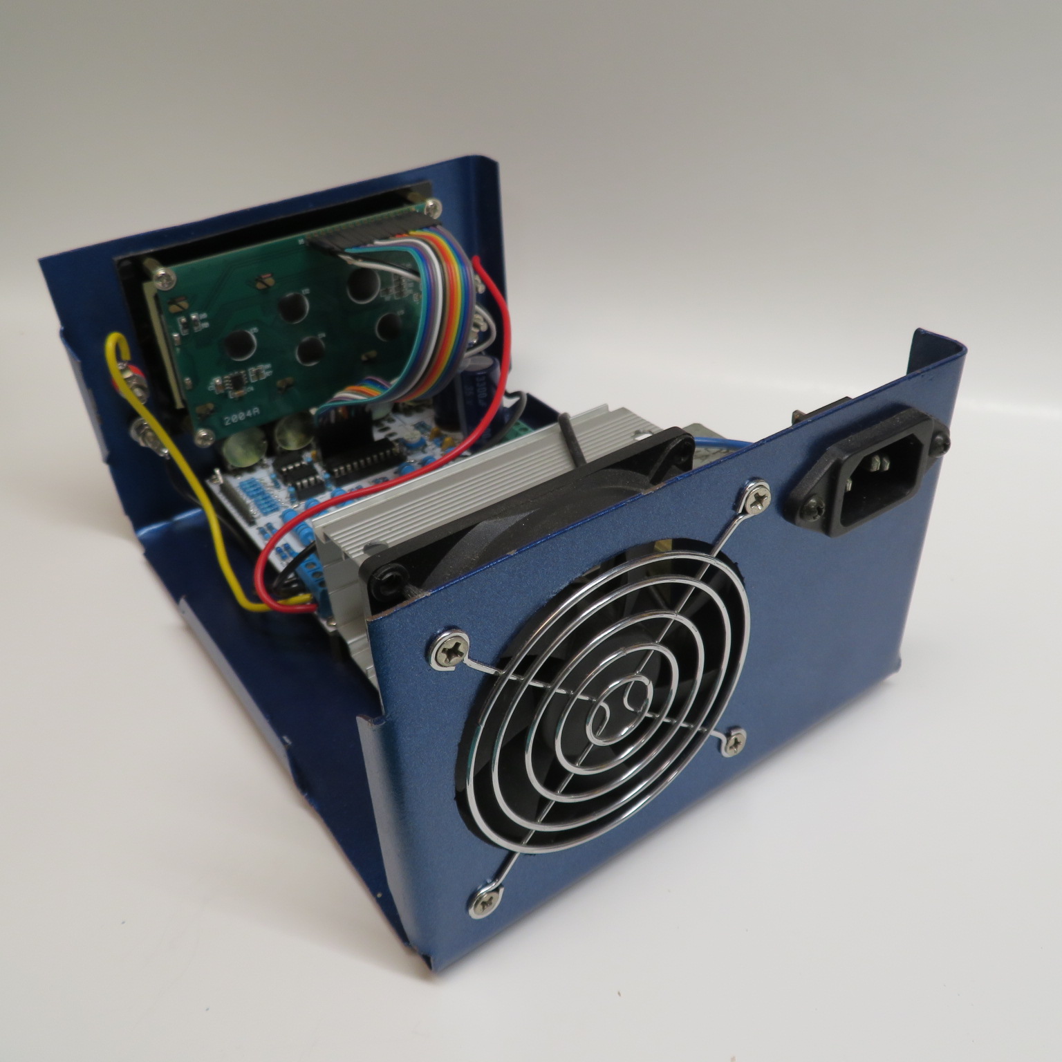
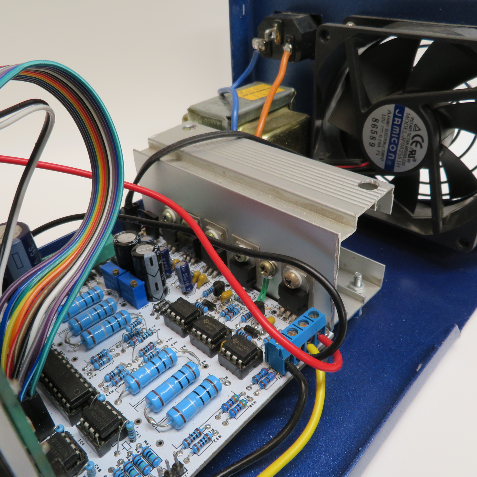
As you can probably see this is a single board design with controls directly mounted on the front, and the heat producing voltage regulation section in the back that can be mounted directly on the heatsink.
I will present here the initial specifications, my design, and explain in detail the problems encountered along the way. Let’s start with the specifications:
Specifications:
- 0V – 40V output (configurable)
- up to 5A current per rail (configurable)
- about %1 accuracy in regulation
- Current limited
- Using the cheapest and most readily available parts
- Small footprint (< 100mm²)
- Single PCB design
- Linear split rail (using audio transformers that I have a pile of)
Let’s briefly address some of these design choices.
0-40V output: This automatically excludes using devices such as LM317 / LM337 for output regulation which max out at 3A and can’t regulate below 1.25V. Going close to 40V at 5A makes it super difficult to chose the output and regulation parts while maintaining a reasonable price point. Parts initially chosen were TIP147 / TIP142 (125W, 10A / 100V transistors) and MC33072 (44V opamps), but even this turned out to be inadequate. See the section on transistor secondary breakdown, bonding wire and thermal limits. It gets really interesting when you push parts to their limits :).
5A output: Besides selecting the right parts (see above) it is difficult to design a small board with the proper trace thickness and separation. At 5A, power trace thickness needs to be around 5mm to handle the current with a modest temperature increase.
1% accuracy: My need didn’t require high accuracy but I was able to achieve ~1% regulation by using 1% resistors and decent components and almost not even trying.
Current limiting: Using a in parallel set of 3, 3W 1% resistors for current sensing, and monitoring the voltage drop across them, with a cheap, readily avaiable opamp in a differential amplifier configuration, turned out to work better than expected.
Cheap parts: This meant aliexpress or ebay chinesium parts, and boy did it bite me in the ass on more than one occasion. More on this later.
Small footprint (100mm²) and single board: This was a cost constraint mainly which made some sense a few years ago, but it is not a wise choice now. It turns out that using a couple of boards doesn’t add much to the overall cost and improves design considerably.
Linear split rail: Based on availability of high power audio transformers that I had laying around.
PSU Operation
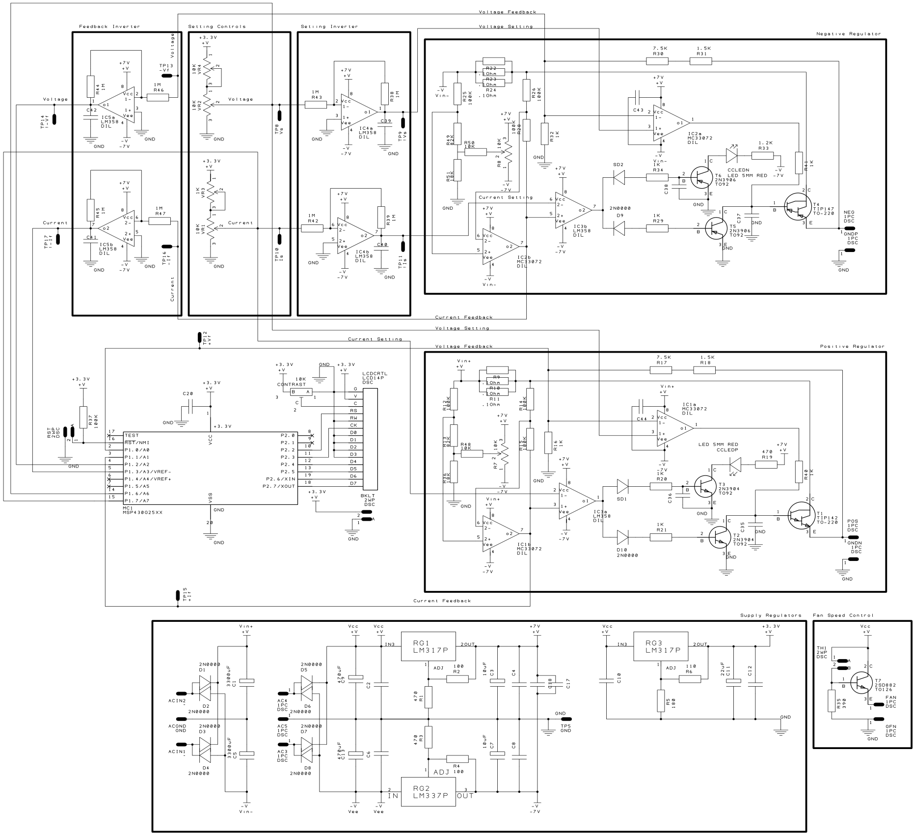
Here’s the schematic for the entire design in PDF format for your download pleasure.
Let’s break it down section by section and talk about what’s happening.
Regulator Section:
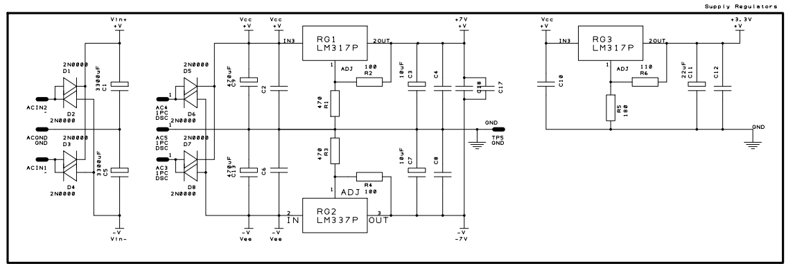
This section uses low cost LM317s / LM337s to create a steady +3.3V supply for the microcontroller and a voltage reference used for regulation, as well as a set of +7V and -7V rails to supply the inversion and current sensing opamps. Resistors R1-R6 set the output voltage.
Most audio transformers have two sets of secondary output windings, one to power the audio amp and another to power low voltage circuits. We use this to our advantage and employ something similar here, so this section also has two bridge rectifiers, one for the output section, and one to power the regulation circuits. This will create a problem with power sequencing which I will describe later.
Ripple capacitors C1 and C2 are selected based on the required voltage and current based on the following table:
First, it becomes painfully obvious that in order to keep the ripple voltage down to a minimum, a very large set of C1/C2 capacitors must be used. This is a big problem with a small PCB footprint.
Second, It is important to note that the maximum PSU output voltage must be lower than the supply voltage minus the ripple voltage. When we factor in the voltage drop of the output transistor, and the maximum operating voltage of the voltage regulation opamps (44V… more on this later) it also becomes very clear that a maximum voltage output of 40V may not be easily achievable.
Voltage and Current Setting and Reference
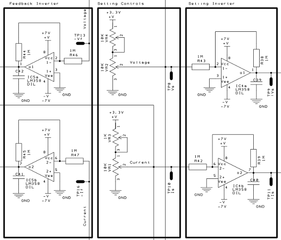
This section is pretty straight forward. A set of 4 pots (VR1-VR4) is used to create the desired voltage output and current limit setting. A coarse and a fine pot is wired in series for easy adjustment.
The setting voltage is compared against the 3.3V reference to generate a specific output voltage. A pair of resistors in the regulation sections divides the output voltage to a range of 0V to 3.3V which is then compared with the setting voltage. The output voltage is adjusted accordingly, so that the divided output voltage always equals the setting voltage. This is the basic principle behind voltage regulation.
This section also includes a voltage inverter for both the setting voltage and the feedback voltage (from the regulator’s voltage divider) which is used in the negative rail of the split supply. The range of the negative voltages is also 0 to -3.3V.
Voltage and Current Regulation
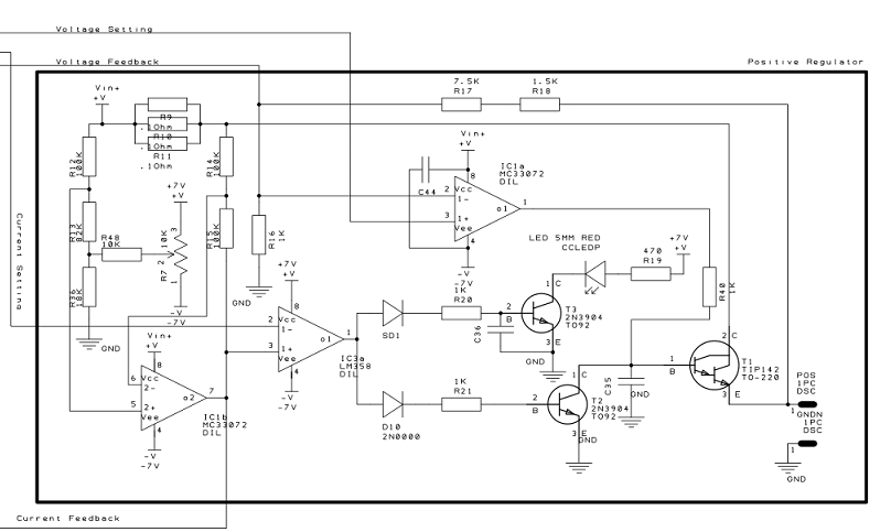
This is the positive voltage regulator. The negative voltage regulator is almost identical, and operates on the same principle but uses PNP parts and negative voltages for setting and feedback.
The voltage regulation is performed by the opamp IC1a. The setting voltage from the pots (could be any other source) is compared against the divider voltage (R16 / R17 + R18) from the output of power darlington transistor T1. The opamp, through opamp action does whatever is necessary to keep the voltage so that the setting equals output. The feedback voltage is also fed back to the MCU so it can be displayed back to the user.
The current regulation is performed in a similar manner. The voltage drop across R9, R10 and R11, is measured using opamp IC1b configured as a differential ampilfier, and fed into opamp IC3a to be compared against the setting voltage. Resistors R12-R15 select the proper current to voltage ratio. A pot (R7) was added to zero the opamp offset so that measurements close to 0 amps are accurate. When IC3a detects that the voltage drop across the current sensing resistors is greater than the current setting voltage, it lowers the base voltage of T1 by pulling it closer to ground via T2 until the measured voltage drop across the current sensing resistors (and thus the current) is lower than the setting. This effectively lowers the supply’s output voltage so that the current limiting setting is satisfied.
A LED is turned on via T3 to indicate that the PSU is in current limiting state. Diode SD1 (Schottky) is selected so that T3 turns on before T2 to keep the LED in a steady state, avoiding flicker as the PSU goes into and out of current protection.
Microcontroller and LCD Display
Using a value line MSP430 microcontroller, we read the voltages for both the setting (from the pots) and the voltage and current feedback. The voltages are then displayed on a Hitachi compatible text lcd matrix display. This MCU has a fairly accurate 10bit ADC and is quite adequate for this project.
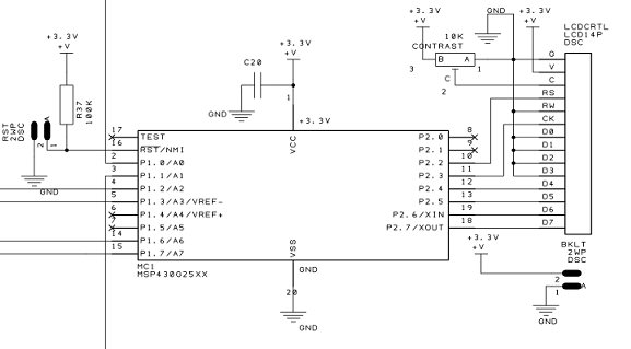
Note that the MCU doesn’t play a role in the regulation or voltage setting process. If the MCU hangs, the PSU will still function as expected, but of course there will be no updates to the LCD display.
The ratios selected for voltage and current feedback and setting via the appropriate resistors in the regulation section, must match the ratio defines in the code, so that the voltage / current measured is the same as the displayed values.
Fan Controller
Given the voltages and current requirements, the output transistors have to be able to dissipate a toasty 125W of power. This requires a massive heatisink… or a small heatsink and a capable fan. We use up the remaining bit of space on the PCB and add a fan controller.
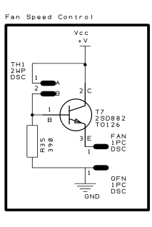
We use a thermistor and an aggressive fan speed curve to keep the heatsink cool. During low power operation the fan will remain off, but a small increase in heatsink temperature will ramp up the fan, quickly cooling it until the fan turns off again or the temperature reaches an equilibrium point. This approach is extremely simple but i works really well in this application.
Design Problems and Lessons Learned
Board Size Constraints
While it’s a good thing to keep a PCB footprint small, it’s not really practical when it comes to power supplies. Power supplies rely on large parts, transistors that require massive heatsinks, a hefty transformer, big capacitors. A decent, high current power supply is going to be big no matter what.
The issue here is that it’s possible to chose cheaper parts and use these parts in parallel trading off increased size for lower cost. The footprint increase in most cases is negligible.
For example, a 6800uF 50V capacitor is going to be big and expensive, but in almost the same space we can install three 3300uF 50V capacitors that are a lot cheaper as a whole. Same goes for a power transistor. A single 300W transistor sells for about $10 (MJ11032 for example), but a set of three 125W transistors will cost about half that, and they will likely perform better as a group.
For that reason, the next iteration of this design will split the PCB into two parts, one will be dedicated for the filtering and power regulation, and another one will handle the controls. This will definitely increase the footprint somewhat. The cost optimization will focus more on the cost of parts rather than a small PCB size.
Single VS Multiple Output Devices
I already touched upon this in the previous section, but it’s almost always more cost effective to use multiple parts in parallel, rather than a single part with higher ratings / specifications.
This is especially true in a power supply design. Replacing a single, large, expensive, and difficult to obtain part with a multiple set of lower rated parts will almost always yield better results when it comes to cost and specs. This can be applied to filter caps, current sensing resistors, and output transistors.
This approach also allows for a high level of customization. If a low power supply is required the same board can be used with fewer, already available parts for at a lower cost. A high power variant can be built by adding additional parts to the group.
Thermal Issues
The worst enemy of a high current power supply is the thermal dissipation. This is especially true when a low voltage, high current setting is required. Let’s say that the transformer used, is a 40VAC RMS transformer that produces a steady 5A of current at 40V DC after rectification and filtering. Let’s also say that only 5V at 5A is required at the output of the PSU. The output transistor in this case will have to dissipate 35V (40V-5V) at 5A, or 175W of power. Now compare that to your soldering iron running a 40W element. The heat sinking capability is going to have to be immense to manage all that heat.
What’s worse is that the performance, and limitations of a power transistor get worse with increased heat. If that heat isn’t removed effectively, a positive feedback loop will surely destroy the output transistor.
A great way to deal with this is to use multiple secondary windings of your transformer (if available). During a low voltage setting, a relay can be used to tap into the low voltage winding of the power transformer reducing the output transistor’s heat dissipation considerably.
Transistor Specifications and Secondary Breakdown
When using power transistors, it is necessary to look beyond the maximum ratings section in the datasheet. Failing to do so will result in a lot of wasted time and destroyed parts. Here’s a maximum rating section of a 300W MJ11032 power transistor:
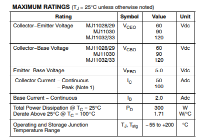
According to this chart, this transistor should be able to handle 120V at 50A. Not a problem then. It satisfies out design specifications by a wide margin.
Well, not quite. Let’s look at the current vs voltage chart further down the datasheet:
While it’s true that the transistor can handle 50A of current, it’s only up to about 7V, and while it’s true that it can handle a voltage of up to 120V, it’s only up to about 0.2A. At 40V, the maximum current for this transistor, is only about 3A. Going beyond that the transistor will be damaged by either burning out the bonding wires, or through secondary breakdown.
This example illustrates that even when using even an expensive, high power transistor, it is quite difficult to achieve the desired specification of 40V at 5A. Unfortunately, more durable transistors are difficult to get and they quickly get expensive. A more realistic 30V at 5A, or 40V at 2A specification is appropriate for this particular transistor, although that is also pretty close to its limits.
It should be clear that to achieve the original specs, it may be a better approach to use multiple output transistors.
Power Sequencing
A power supply Achilles heel is its ability to regulate voltage during the power up and power down sequence. Many stories of expensive devices and ICS damaged by badly designed power supplies on start-up come to mind. Some power supplies also tend to overshoot when they enter or exit the current limit mode (I have one of these commerical products myself)
We can all agree that having a power supply on your bench that damages your equipment is pretty useless. If there is one thing that you have to be able to trust it’s your power supply and your multimeter. The inability of your PSU to manage regulation is caused by the various sections of the PSU not starting up, or shutting down in the proper sequence.
You want to bring up your regulation section first, before the power section is ready. If the opamps don’t have a stready supply then may misbehave driving the output section wild destroying whatever is attached to the output of the PSU.
Consider then the power down sequence. Again, you want the regulation section to power down last. But we have all these large caps in the output section that are holding on to the electrons.
This is actually quite a difficult problem to deal with. This design here is susceptible to power down overshoots because the regulation section’s rails, especially the 7V rails power down unevenly.
This can be addressed by adjusting the value of the filter capacitors on the 3.3V, 7V and -7V rails, but this has to be addressed each time the design is modified.
The most effective way to address this is to add an additional voltage monitor and relay to prevent any overshoot from reaching an external device. This will be added to subsequent designs.
Quality and Source of Components
I’m going to try to keep this section short otherwise I’ll just get angry. A lot of parts on Ebay or Aliexpress are fake. They can be either re-labeled lower spec parts, parts that failed QC in the factory, or just broken junk that doesn’t work at all.
This applies to everything but it’s especially common when it comes to capacitors, power transistors, and even opamps. Usually a low cost part compared to a western counterpart is the giveaway.
I once spent a month troubleshooting a problem with generated video which would streak and smear on a simple 5 transistor circuit that ended up being a crappy transistors (2s9034 / 2s9036) that can’t switch pixels beyond 1Mhz (~200MHz spec).
How desperate must you be, to produce a shitty transistor which is common as dirt. None of the Chinese made 2n9034 transistors I tried (from multiple sources) worked as expected. I have had a similar issues with TL074 opamps that have 10% of the specified slew rate compared to a western product. Garbage…
During the design phase I strongly recommend using parts from reputable sources. Chinese resistors though, seem to be pretty good. Never had an issue there.
Conclusions
While this design works quite well and has proven to be quite durable, the following changes will be made to subsequent designs:
- Create a separate power regulation and control boards
- Use input relay to switch to lower voltage secondary when low voltage is required
- Use output relay to prevent overshoot and power sequencing issues, and to prevent faulty output from damaging external equipment
- Use multiple power transistors to increase power capability
- Use multiple filter caps to reduce costs and allow greater design flexibility.
- Create additional control board that doesn’t use pots but a microcontroller to set and monitor regulation.